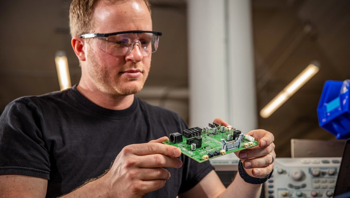
A PCB layout refers to the physical design or arrangement of electronic components and their interconnections on a printed circuit board (PCB). PCB layout is a critical step in the design of electronic circuits, as it directly impacts the performance, reliability, and cost of the final product.
What is PCB design?
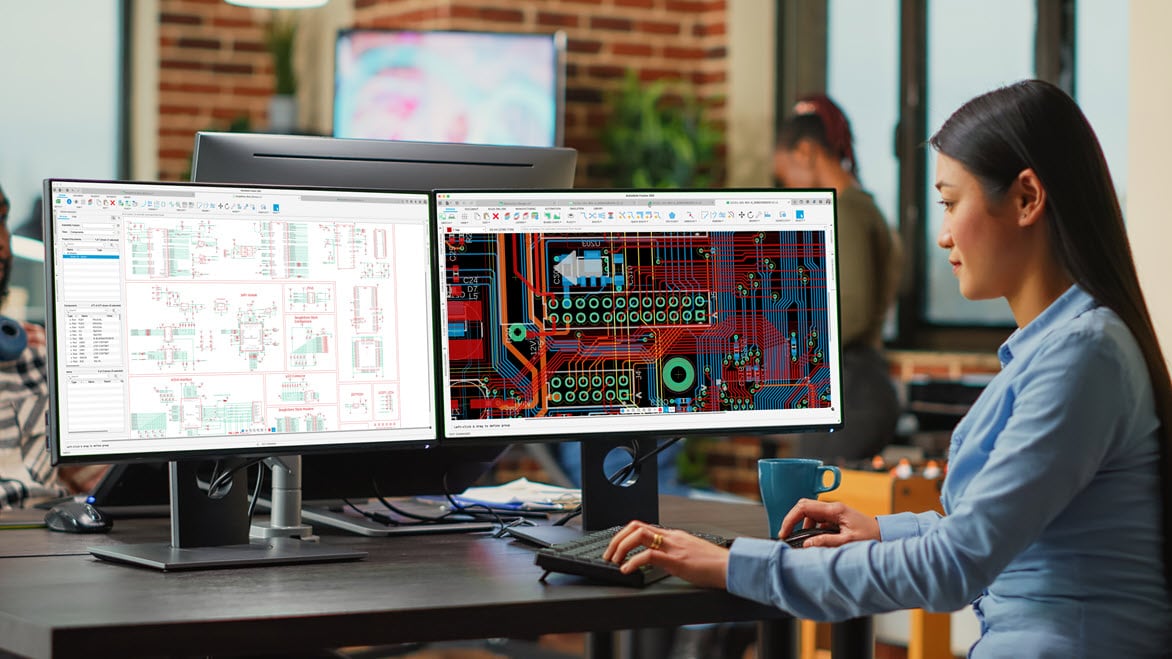
Printed circuit board (PCB) design is the process of bringing your electronic circuit boards to life in their physical form. Printed circuit boards (PCBs) are used in a wide variety of electronic devices, from small consumer products to large industrial machines.
The goal of PCB design is to create functional, reliable, cost-effective circuit boards that meet the electrical and physical requirements of the devices they will be used in. PCB design is also critical to make sure devices function properly and minimize the risks of electrical shorts, interference, and other problems that can arise with poorly designed circuits.
What is PCB design software?
PCB design software is a computer program used to design and create printed circuit boards (PCBs). PCB design software allows users to create a layout for a circuit board, including placing components and routing connections between them. The software can also be used to make sure that the layout meets design requirements, including trace width and clearance between components.
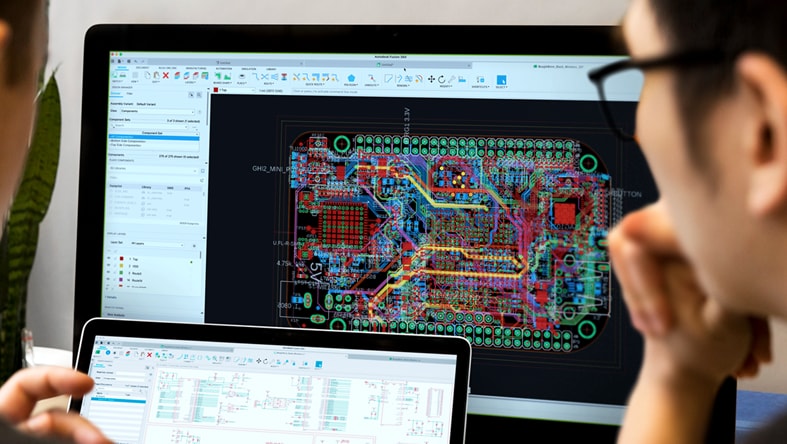
How to design a PCB using Fusion 360
To create a PCB in Fusion 360 electronics, launch the software and open the electronic design module from the file drop-down menu. Here, you'll find all the necessary tools for designing your schematic and board layout professionally. You can begin by creating a schematic and use the extensive library of components to add the required parts to your design. Fusion 360 electronics enables easy component placement and connectivity, for a streamlined design process.
Benefits of PCB design software
Improved accuracy
Make sure that circuit boards are designed with a high level of accuracy. Reduce the risk of errors and improve product reliability with electronics simulation.
Increased flexibility
Eliminate the need for physical prototypes, reducing costs and design iterations by easily modifying the design directly in the software.
Better collaboration
Multiple designers and cross-functional teams can work on a design concurrently reducing design time and improving product quality.
Time and cost savings
Features such as interactive routing, schematic capture, and component libraries reduce design time. PCB design software also reduces the cost of production by optimizing the placement of components, reducing the circuit board size, and more.
PCB design process
Electronic component placement
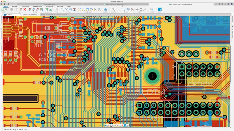
The PCB design process begins by converting an electronics schematic diagram into a physical circuit board layout. Then it’s time to put your problem solving skills to the test by placing electrical components within a tightly constrained space.
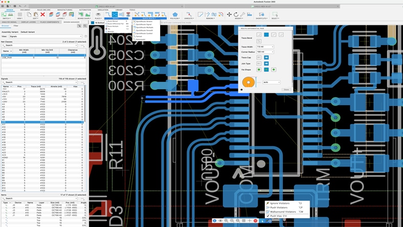
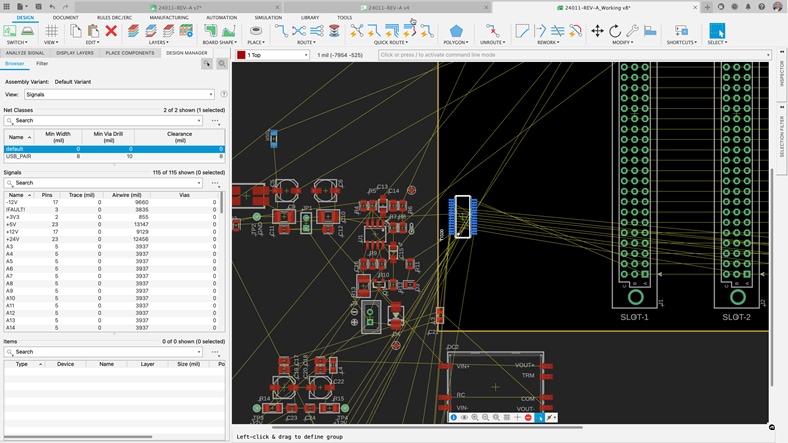
PCB routing
The PCB routing process is both an art and a science. Using physical wires, you’ll define electrical connectivity between components on a PCB layout. No two circuit boards are the same, the routing is what makes your design unique.
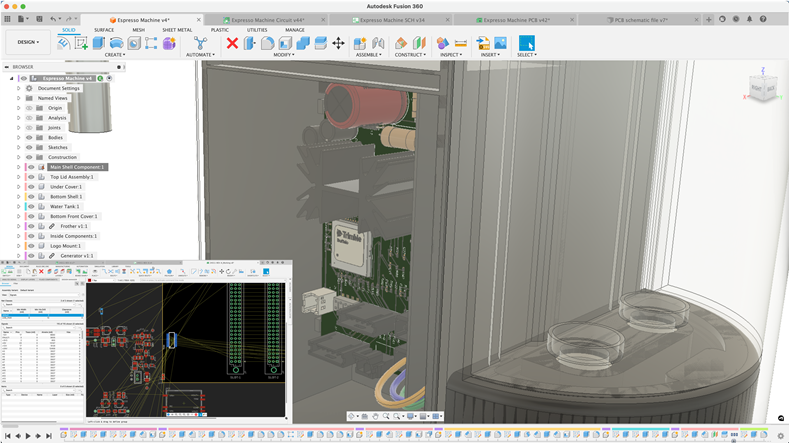
ECAD-MCAD integration
Nearly every PCB design exists within a mechanical product. Using Fusion 360 native ECAD & MCAD makes it easy for electronics and mechanical engineers to concurrently work on the same design to validate product fit, form, and function.
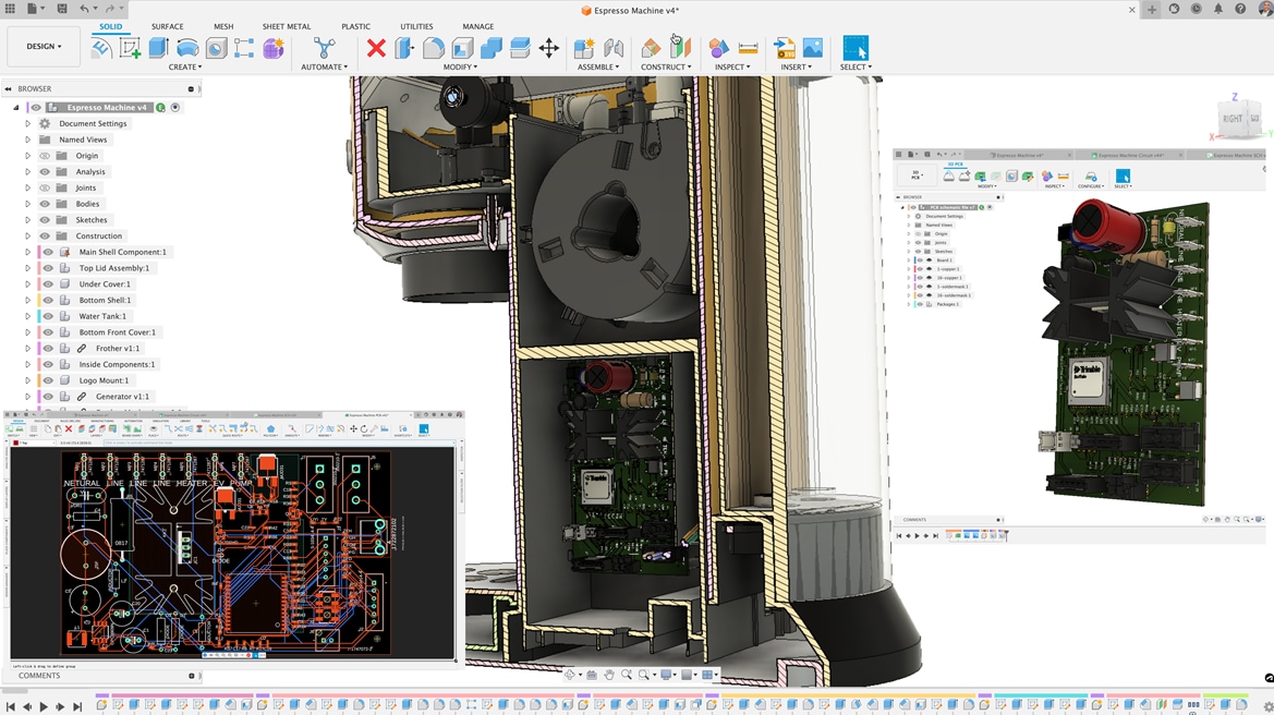
Where mechanical meets electrical design
Intelligent products require integrated electrical and mechanical characteristics. Learn how to seamlessly share design changes and collaborate between mechanical and electrical workflows in Autodesk Fusion 360.
PCB design basics
Get started with PCB design software with these tutorials, articles, and tips.
What's a PCB?
Learn about the construction of a PCB (printed circuit board) and how they fit into today’s world of advanced electronic devices.
PCB layout basics
Learn how to convert a circuitry schematic design to a PCB layout and begin placing your electronic components.
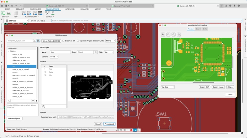
PCB manufacturing
Learn how to produce manufacturing data for a printed circuit board using the CAM processor in the PCB editor.
PCB design resources
Learn the basics of how to work with 3D PCB design in Fusion 360. Get answers to some of the most commonly asked questions from the electronics community.
Design your printed circuit board (PCB) layout with these tips for routing, component placement, heat dissipation, and more.
Moisture, humidity, dust? No problem! Here are the main considerations that you need to make when designing PCBs that will live in harsh environments.
Learn how the Fusion 360 Signal Integrity Extension improves product compliance and performance, reduces costly physical PCB testing and prototyping, and accelerates high-speed PCB development.
This PCB design advice that will help you lower costs, have fewer production failures, and improve product quality.
PCB design revisions used to be costly and time-consuming. Not anymore! Here’s why PCB designers need 3D modeling software.
PCB design software FAQs
Factors to consider when choosing PCB design software includes:
- Functionality
- Ease of use
- Compatibility
- Cost
- Community and learning resources.
Autodesk Fusion 360 is an affordable fully integrated electronics design and manufacturing software.
Yes, Autodesk Fusion 360 offers collaboration features that allow multiple users to work on the same design simultaneously. They can share design files, and communicate in the same software environment in real-time. Collaboration features include version control, commenting, and real-time collaboration.
Yes, PCB simulation software allows you to test and validate the functionality and performance of your design without having to physically build and test a prototype.
File formats for PCB design include, Gerber, ODB++, dwg, pick and place file, BOM, dxf, nc drill file, IPC netlist, Sch and PCB files, SPICE models, IBIS, and BSDL.
If your schematics are made with EAGLE all you have to do is to open them in Fusion 360 electronics, there is no import process needed. Create a project folder and upload them.
See more FAQ
See less FAQ